
As semiconductor devices continue evolving toward higher power density, smaller geometries, advanced packaging, and AI-driven computing architectures, thermal reliability validation has become more critical than ever.
Modern semiconductor products are no longer exposed to stable operating environments. Instead, they frequently experience rapid temperature fluctuations caused by:
- AI workload changes
- High-speed data processing
- Power cycling
- Automotive operating environments
- Outdoor telecommunications systems
- Advanced chiplet integration
- Silicon photonics thermal variation
These repeated temperature changes generate thermo-mechanical stress inside semiconductor packages.
To evaluate long-term reliability under such conditions, manufacturers rely heavily on environmental testing systems capable of controlled thermal cycling and fast temperature transitions.
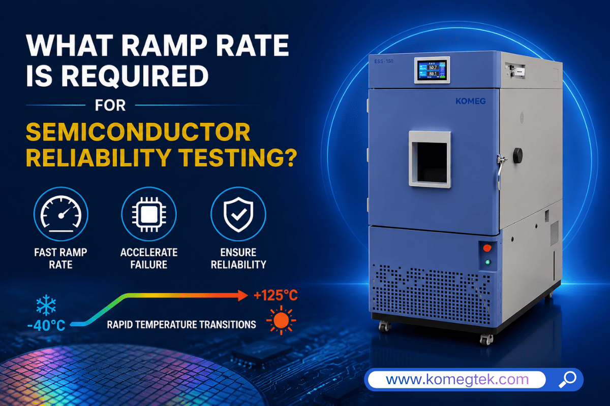
One of the most important parameters in semiconductor reliability testing is ramp rate.
Ramp rate directly affects:
- Thermal stress intensity
- Failure acceleration
- Test realism
- Semiconductor package fatigue
- Reliability validation effectiveness
This article explains:
- What does ramp rate mean
- Typical ramp rate requirements
- How ramp rate affects semiconductor reliability
- Industry standards and applications
- Failure mechanisms accelerated by fast ramp testing
- Differences between standard cycling and rapid thermal transition testing
- How to select the correct ramp rate for semiconductor testing
What Is Ramp Rate in Environmental Testing?
Ramp rate refers to the speed at which an environmental chamber changes temperature over time.
It is typically measured in:
- °C/min
- °F/min
For example:
- A chamber changing from 25°C to 125°C in 10 minutes operates at 10°C/min.
- A chamber changing from -40°C to +125°C in 15 minutes operates at approximately 11°C/min.
Ramp rate is one of the most critical specifications in semiconductor environmental testing because it determines how aggressively thermal stress is applied to the device under test (DUT).
Faster ramp rates create larger thermal gradients and more severe mechanical stress inside semiconductor packages.
Why Ramp Rate Matters in Semiconductor Reliability Testing
Semiconductor devices contain multiple materials with different coefficients of thermal expansion (CTE), including:
- Silicon dies
- Copper interconnects
- Organic substrates
- Mold compounds
- Underfill materials
- Solder joints
- Thermal interface materials
When temperatures change rapidly, these materials expand and contract at different rates.
This creates thermo-mechanical stress at internal interfaces.
The faster the temperature transition, the greater the stress intensity.
Ramp rate, therefore, plays a major role in accelerating:
- Solder fatigue
- Delamination
- Wire bond damage
- Package cracking
- Substrate warpage
- Optical alignment drift
- Thermal interface degradation
This is especially important in modern advanced semiconductor packaging technologies.
Typical Ramp Rate Requirements for Semiconductor Testing
Ramp rate requirements vary depending on:
- Device type
- Industry standard
- Package structure
- Reliability objective
- Application environment
Typical semiconductor testing ramp rates include:
Standard Thermal Cycling
Typical ramp rates:
- 1°C/min to 5°C/min
Used for:
- Conventional JEDEC thermal cycling
- Consumer electronics
- Long-duration reliability studies
These slower transitions simulate normal operational conditions.
Fast Ramp Rate Testing
Typical ramp rates:
- 5°C/min to 15°C/min
Used for:
- Accelerated reliability testing
- Semiconductor package validation
- AI processor testing
- Automotive electronics
- Silicon photonics systems
Fast ramp testing significantly accelerates fatigue mechanisms.
Highly Accelerated Thermal Stress Testing
Typical ramp rates:
- 15°C/min to 30°C/min or higher
Used for:
- HALT testing
- Failure analysis
- Extreme reliability validation
- Advanced semiconductor package screening
These aggressive profiles create severe thermo-mechanical stress.
Why Advanced Semiconductor Packaging Requires Faster Ramp Rates
Modern semiconductor technologies are becoming increasingly sensitive to thermal stress.
Advanced packaging structures now include:
- Chiplets
- 2.5D integration
- 3D IC stacking
- Silicon interposers
- HBM memory integration
- Co-Packaged Optics (CPO)
These highly integrated architectures create:
- Larger thermal gradients
- Higher localized power density
- More complex mechanical stress distribution
Traditional low ramp rate testing may no longer sufficiently reproduce real-world thermal conditions.
AI accelerators and high-performance GPUs can experience extremely rapid temperature variation during operation.
Fast ramp rate testing, therefore, becomes essential for evaluating realistic reliability behavior.
Ramp Rate and Semiconductor Failure Mechanisms
Solder Joint Fatigue
Solder fatigue is one of the most common thermal reliability failures.
Rapid temperature changes repeatedly strain solder connections until cracks form.
Higher ramp rates accelerate fatigue accumulation.
This is especially critical in:
- BGA packages
- Flip-chip devices
- Large AI processors
- Automotive power electronics
Delamination
Fast temperature transitions may weaken bonding interfaces between dissimilar materials.
Delamination can occur between:
- Mold compounds
- Underfill layers
- Die attach materials
- Substrates
Once delamination begins, reliability degradation often accelerates rapidly.
Package Cracking
Aggressive thermal gradients may generate excessive internal stress.
This can eventually lead to:
- Mold cracking
- Die cracking
- Structural package failure
Large advanced semiconductor packages are particularly vulnerable.
Wire Bond Damage
Repeated thermal expansion and contraction can fatigue delicate wire bonds.
This may result in:
- Increased electrical resistance
- Intermittent failure
- Open circuits
Substrate Warpage
Fast thermal transitions may deform large semiconductor substrates.
Warpage is becoming increasingly important in:
- AI accelerators
- High-density chiplet systems
- Silicon photonics modules
- Large GPU packages
Even a small deformation can affect long-term reliability.
Ramp Rate Requirements in Different Industries
Automotive Electronics
Automotive semiconductors experience extreme environmental conditions.
AEC-Q100 qualification often requires aggressive thermal cycling profiles to simulate:
- Engine heat
- Outdoor winter conditions
- Frequent startup cycles
Automotive reliability testing frequently uses higher ramp rates than consumer electronics testing.
AI and High-Performance Computing
AI servers generate highly dynamic thermal conditions.
GPU workloads can rapidly shift from idle to peak power operation.
This creates fast thermal variation inside semiconductor packages.
Fast ramp rate testing helps reproduce these operating conditions.
Silicon Photonics and CPO
Co-Packaged Optics systems are highly sensitive to thermal expansion mismatch.
Even microscopic alignment shifts may affect:
- Optical coupling
- Signal integrity
- BER performance
Fast ramp testing helps evaluate optical stability under aggressive thermal conditions.
Aerospace and Defense
Military and aerospace electronics often require extended reliability validation under severe environmental conditions.
Fast thermal transitions may simulate:
- High-altitude temperature swings
- Rapid environmental exposure
- Harsh operational conditions
Ramp Rate vs Thermal Shock Testing
Although both involve rapid temperature change, fast ramp rate testing and thermal shock testing are different.
Fast Ramp Rate Chambers
Use controlled continuous temperature transitions.
Advantages:
- Better temperature control
- Realistic thermal cycling
- Lower thermal overshoot
- Better optical monitoring compatibility
Commonly used for:
- Semiconductor reliability testing
- AI hardware validation
- Silicon photonics testing
Thermal Shock Chambers
Use separate hot and cold zones with near-instantaneous transfer.
Advantages:
- More aggressive stress
- Faster fatigue acceleration
- Severe CTE mismatch evaluation
Commonly used for:
- Package robustness testing
- Solder fatigue analysis
- Automotive qualification
Both methods are important for semiconductor reliability validation.
Why Temperature Uniformity Matters During Fast Ramp Testing
High ramp rates make temperature uniformity increasingly difficult.
Poor airflow design may create:
- Hot spots
- Cold zones
- Uneven thermal gradients
Localized temperature differences can produce inconsistent stress conditions across devices.
This may result in unreliable or non-repeatable test data.
Advanced semiconductor chambers, therefore require:
- Optimized airflow engineering
- High-efficiency circulation systems
- Precise PID temperature control
- Stable refrigeration performance
Temperature uniformity becomes even more critical for:
- Large DUTs
- Multi-chip assemblies
- Optical communication modules
- Wafer-level testing
Refrigeration Requirements for High Ramp Rate Chambers
Fast cooling transitions require advanced refrigeration systems.
Most high-performance semiconductor chambers use:
- Cascade refrigeration systems
- Multi-stage compressors
- High-capacity heat exchangers
These systems provide:
- Rapid pull-down performance
- Stable low-temperature operation
- Precise temperature recovery
- Long-duration reliability
Efficient refrigeration engineering is essential for maintaining stable ramp performance.
Common Ramp Rate Challenges in Semiconductor Testing
Thermal Overshoot
Aggressive ramp rates may create temperature overshoot.
Sensitive semiconductor devices may be damaged if chamber control is unstable.
Inconsistent Device Temperature
Large devices may heat unevenly during rapid transitions.
This may affect test accuracy.
Airflow Disturbance
Poor chamber airflow can reduce temperature uniformity during fast transitions.
Excessive Mechanical Stress
Extremely aggressive ramp rates may create unrealistic stress conditions.
The objective should be accelerated realism, not unrealistic destruction.
How to Select the Right Ramp Rate
Choosing the correct ramp rate depends on several factors.
Device Type
Larger packages may require different thermal profiles than small ICs.
Reliability Objectives
Qualification testing may require different ramp rates than failure analysis.
Industry Standards
Automotive, aerospace, and semiconductor standards may specify thermal cycling requirements.
Package Sensitivity
Optical and advanced packaging technologies may require carefully controlled transitions.
Test Duration
Higher ramp rates accelerate stress but may also increase chamber complexity and operating cost.
Environmental Chambers Used for Fast Ramp Rate Testing
Common chamber types include:
Fast Ramp Rate Chambers
Designed specifically for rapid temperature transitions.
Thermal Cycling Chambers
Used for long-duration temperature reliability testing.
Thermal Shock Chambers
Used for aggressive package stress evaluation.
Temperature Humidity Chambers
Used for combined thermal and humidity reliability validation.
Future Trends in Semiconductor Ramp Rate Testing
As semiconductor technologies continue evolving, ramp rate requirements will become increasingly demanding.
Future trends include:
- Higher AI chip power density
- More advanced packaging structures
- Silicon photonics adoption
- Chiplet integration
- Higher-speed optical interconnects
- Increased thermal stress sensitivity
Future environmental chambers will require:
- Faster ramp capability
- Improved temperature uniformity
- Smarter PID control
- AI-assisted diagnostics
- Better airflow engineering
- Enhanced energy efficiency
Environmental reliability testing will remain one of the most important validation processes in semiconductor manufacturing.
Ramp rate is one of the most critical parameters in semiconductor reliability testing because it directly influences thermo-mechanical stress intensity and failure acceleration.
As semiconductor technologies evolve toward:
- AI accelerators
- Chiplet architectures
- Silicon photonics
- Automotive electronics
- High-density packaging
thermal reliability validation becomes increasingly complex.
Fast ramp rate testing helps engineers reproduce realistic operating stress conditions while accelerating long-term fatigue mechanisms.
However, selecting the correct ramp rate requires balancing:
- Realism
- Acceleration
- Device sensitivity
- Industry standards
- Reliability objectives
Modern semiconductor environmental chambers must provide:
- Precise temperature control
- Stable rapid transitions
- Excellent temperature uniformity
- Reliable refrigeration systems
- Long-duration operational stability
KOMEG provides advanced, fast-ramp-rate environmental chambers designed for semiconductor, AI infrastructure, automotive electronics, and silicon photonics reliability testing applications.