
Modern semiconductor devices are becoming smaller, faster, and more powerful than ever before. From AI accelerators and automotive control systems to silicon photonics and advanced chiplet architectures, today’s semiconductor packages operate under increasingly harsh thermal conditions.
As computing power increases, thermal stress inside semiconductor devices also rises dramatically.
Rapid temperature fluctuations generated during operation, power cycling, transportation, manufacturing, and environmental exposure can gradually damage semiconductor packages over time.
To ensure long-term reliability, manufacturers rely heavily on thermal shock testing.
Thermal shock testing is one of the most critical accelerated reliability validation methods used throughout the semiconductor industry. It helps engineers identify hidden weaknesses in semiconductor packaging before products reach the market.
This article explains:
- What thermal shock testing is
- Why it matters for semiconductor reliability
- Common failure mechanisms
- Key JEDEC and automotive standards
- Thermal shock chamber requirements
- Applications in AI, automotive, and advanced packaging
- How thermal shock testing improves product lifespan and reliability
What Is Thermal Shock Testing?
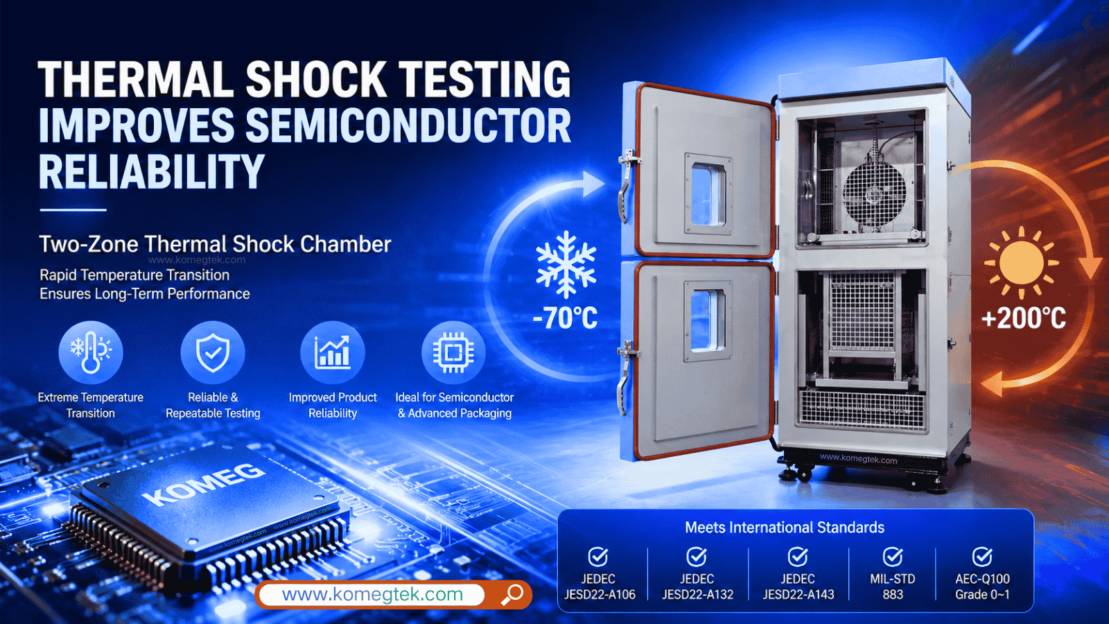
Thermal shock testing is an accelerated environmental stress test that rapidly exposes semiconductor devices to alternating extreme hot and cold temperatures.
Unlike standard thermal cycling, thermal shock testing subjects components to sudden temperature transitions with minimal transfer time between temperature zones.
The objective is to create severe mechanical stress caused by rapid thermal expansion and contraction.
This testing helps engineers identify package weaknesses that may eventually lead to field failures.
Thermal shock testing is widely used for:
- Semiconductor package qualification
- Automotive electronics validation
- Military and aerospace electronics
- AI chip reliability testing
- Advanced packaging evaluation
- Optical communication device testing
Industry standards such as JEDEC JESD22-A143 and JESD22-A106 define thermal shock testing procedures for semiconductor reliability validation.
Why Semiconductor Devices Are Vulnerable to Thermal Stress
Semiconductor packages contain multiple materials with different coefficients of thermal expansion (CTE).
Common materials include:
- Silicon dies
- Copper interconnects
- Organic substrates
- Ceramics
- Mold compounds
- Solder joints
- Adhesives
When temperature changes occur rapidly, each material expands and contracts at different rates.
This creates mechanical stress at material interfaces.
Over repeated thermal shock cycles, this stress may cause:
- Solder fatigue
- Delamination
- Package cracking
- Wire bond failure
- Die attach separation
- Substrate warpage
Advanced semiconductor packages are especially sensitive because they use increasingly complex heterogeneous integration structures.
Thermal Shock vs Thermal Cycling
Although thermal shock and thermal cycling are often discussed together, they are not the same test.
Thermal cycling uses gradual temperature transitions to simulate real operating environments.
Thermal shock testing uses extremely rapid transitions between hot and cold conditions to create much more aggressive stress.
Thermal shock, therefore, accelerates failure mechanisms more quickly.
According to semiconductor reliability testing references, thermal shock is considered one of the most severe temperature-related reliability tests for electronic packaging.
Why Thermal Shock Testing Is Important for Semiconductor Reliability
Identifying Early Package Failures
One major objective of thermal shock testing is to expose latent manufacturing or material defects before products enter mass production.
Accelerated stress testing helps engineers identify:
- Weak solder joints
- Poor die attach integrity
- Material incompatibility
- Packaging process issues
Texas Instruments notes that accelerated reliability testing is essential because semiconductor devices cannot realistically be observed under normal operating conditions for many years before release.
Evaluating Material Compatibility
Modern semiconductor packaging combines many advanced materials inside extremely compact structures.
Thermal shock testing helps validate whether these materials can withstand repeated thermal expansion mismatch without structural degradation.
This is increasingly important for:
- Chiplet architectures
- 2.5D packaging
- 3D IC integration
- Silicon photonics
- High-power AI processors
Improving Long-Term Reliability
Thermal shock testing compresses years of operational stress into a shorter testing timeframe.
By exposing potential weaknesses early, manufacturers can improve:
- Product lifespan
- Field reliability
- Safety performance
- Warranty risk reduction
This is especially critical in automotive and aerospace electronics, where failures can create severe safety risks.
Common Failure Mechanisms Revealed by Thermal Shock Testing
Solder Joint Fatigue
Solder joints are among the most vulnerable structures during rapid thermal transitions.
Repeated expansion and contraction gradually weaken solder connections until cracks form.
Solder fatigue is one of the most common semiconductor packaging failures detected during thermal shock testing.
Package Cracking
Rapid temperature changes may create excessive mechanical stress inside package materials.
This can eventually lead to:
- Mold compound cracking
- Die cracking
- Internal structural damage
Package cracking may not always be immediately visible but can eventually cause catastrophic failure.
Delamination
Delamination occurs when bonded material layers begin separating due to thermal stress.
This may occur between:
- Die attach layers
- Substrates
- Underfill materials
- Mold compounds
Once delamination begins, moisture ingress and mechanical instability may rapidly accelerate failure.
Wire Bond Failure
Repeated thermal shock stress may damage delicate wire bonds connecting semiconductor dies to package leads.
Bond wire fatigue can cause:
- Electrical instability
- Increased resistance
- Open circuits
Substrate Warpage
Large advanced packages may deform under repeated thermal shock exposure.
Warpage becomes increasingly problematic in:
- AI accelerators
- High-performance GPUs
- Large chiplet systems
- Advanced photonic packages
Even slight deformation may affect long-term reliability.
Thermal Shock Testing in AI and High-Performance Computing
AI infrastructure is creating new semiconductor reliability challenges.
Modern AI chips generate:
- Extremely high power density
- Rapid thermal fluctuations
- Continuous workload variation
This creates aggressive thermal stress conditions inside semiconductor packages.
As AI processors continue scaling upward in power consumption, thermal shock reliability validation becomes increasingly important.
Advanced packaging technologies used in AI systems are particularly vulnerable to CTE mismatch and thermal fatigue.
Thermal Shock Testing for Automotive Electronics
Automotive semiconductor reliability requirements are among the strictest in the industry.
Automotive chips must withstand:
- Extreme outdoor temperatures
- Frequent power cycling
- Long service lifetimes
- Harsh vibration environments
AEC-Q100 automotive qualification standards often require hundreds or thousands of thermal shock cycles.
Automotive applications relying heavily on thermal shock testing include:
- ADAS systems
- EV battery management
- Autonomous driving electronics
- Power modules
- Radar systems
Reliability expectations for automotive electronics are extremely high because failures may directly affect vehicle safety. Community discussions among engineers frequently highlight the increasing complexity of ensuring reliability in advanced automotive chips.
Thermal Shock Testing Standards for Semiconductor Reliability
JEDEC Standards
JEDEC defines many of the semiconductor industry’s most widely used reliability testing procedures.
Important thermal shock-related standards include:
- JESD22-A106
- JESD22-A132
- JESD22-A143
These standards define:
- Temperature ranges
- Transfer times
- Soak durations
- Cycle counts
- Failure criteria
JEDEC standards help ensure repeatability and consistency across semiconductor qualification programs.
MIL-STD Standards
Military-grade semiconductors often follow MIL-STD-883 thermal shock procedures.
These tests typically use wider temperature ranges and stricter reliability requirements.
Military applications require exceptional long-term durability under harsh environmental conditions.
AEC-Q100 Automotive Qualification
AEC-Q100 is one of the most important reliability standards for automotive semiconductors.
Thermal shock testing under AEC-Q100 often includes:
- -65°C to +150°C testing
- 500 to 1000 cycles or more
- Detailed post-test failure analysis
These tests validate long-term automotive reliability performance.
Thermal Shock Chamber Requirements
High-performance semiconductor reliability testing requires highly specialized thermal shock chambers.
Key chamber requirements include:
Rapid Temperature Transfer
Thermal shock chambers must rapidly move devices between hot and cold zones with minimal delay.
Fast transfer times are critical for creating aggressive thermal stress.
Precise Temperature Control
Accurate temperature control ensures consistent stress conditions and repeatable test results.
Poor temperature control may create unrealistic or inconsistent failure behavior.
Excellent Temperature Uniformity
Uniform chamber conditions prevent localized stress variations across test samples.
This is especially important for:
- Large semiconductor packages
- Multi-chip modules
- Optical communication devices
Long-Term Operational Stability
Semiconductor qualification programs often require:
- Hundreds of cycles
- Thousands of cycles
- Continuous long-duration operation
Reliable chamber stability is essential for valid test data.
Air-to-Air vs Liquid Thermal Shock Chambers
Thermal shock systems are generally divided into:
Air-to-Air Thermal Shock Chambers
These systems use separate hot and cold air zones.
They are commonly used for:
- Semiconductor packaging
- Electronics reliability testing
- Optical module testing
Air-to-air systems offer cleaner and more controlled testing environments.
Liquid Thermal Shock Systems
Liquid systems use heated and cooled fluids for faster heat transfer.
These systems create even more severe thermal stress conditions.
Liquid thermal shock testing is sometimes used for specialized high-reliability applications.
Thermal Shock Testing in Advanced Semiconductor Packaging
Advanced packaging technologies are making thermal reliability increasingly complex.
Modern semiconductor packages now include:
- Chiplets
- 2.5D integration
- 3D stacking
- Silicon interposers
- Heterogeneous integration
These structures create concentrated thermal gradients and mechanical stress.
Research on advanced packaging increasingly emphasizes the importance of thermal-aware reliability engineering to reduce stress-related failures.
Thermal shock testing is therefore becoming more important throughout next-generation semiconductor development.
Why Environmental Testing Matters More Than Ever
Semiconductor devices are now used in increasingly demanding environments:
- AI data centers
- Electric vehicles
- Aerospace systems
- Autonomous machines
- 5G infrastructure
- Silicon photonics systems
Failures in these applications can result in:
- Massive financial losses
- Safety risks
- System downtime
- Data loss
Environmental reliability testing helps manufacturers reduce these risks before deployment.
Future Trends in Semiconductor Thermal Reliability Testing
As semiconductor technology evolves, thermal reliability testing requirements will continue expanding.
Future trends include:
- Higher power density chips
- Faster thermal transitions
- Larger advanced packages
- AI-driven workload variation
- More complex heterogeneous integration
Next-generation thermal shock chambers will increasingly require:
- Faster transfer speeds
- Improved temperature uniformity
- Enhanced airflow engineering
- AI-assisted predictive diagnostics
- Real-time monitoring systems
Reliability testing will remain one of the most critical processes in semiconductor manufacturing.
Thermal shock testing plays a vital role in improving semiconductor reliability by exposing devices to aggressive temperature stress conditions that accelerate failure mechanisms.
From solder fatigue and delamination to package cracking and substrate warpage, thermal shock testing helps engineers identify weaknesses before products reach real-world applications.
As semiconductor technologies continue evolving toward:
- AI computing
- Chiplet architectures
- Silicon photonics
- Automotive electronics
- Advanced packaging
thermal reliability validation becomes increasingly important.
Industry standards such as JEDEC, MIL-STD, and AEC-Q100 provide structured qualification frameworks that help manufacturers ensure long-term semiconductor durability and operational stability.
High-performance thermal shock chambers with rapid transfer capability, precise temperature control, and excellent uniformity are now essential tools throughout the semiconductor industry.
KOMEG provides advanced environmental testing solutions for semiconductor reliability validation, including:
designed to meet the demanding reliability requirements of next-generation semiconductor technologies.