
Driven by the continuous advancement of artificial intelligence (AI), hyperscale data centers, cloud computing, and high-performance networking infrastructure, the global demand for high-speed, energy-efficient data transmission technologies has grown exponentially. Traditional copper-based interconnection architectures have gradually reached inherent physical limits in terms of bandwidth density, power efficiency, and signal integrity. To break through these technical bottlenecks, the semiconductor industry is increasingly adopting Co-Packaged Optics (CPO) as a core solution.
CPO technology embeds optical engines in the same package or substrate alongside switching ASICs and AI processors. This innovative architectural design significantly shortens electrical transmission paths, cuts power consumption, enhances bandwidth scalability, and lays a solid technical foundation for next-generation AI infrastructure. Nevertheless, the heterogeneous integration of lasers, silicon photonic integrated circuits (PICs), fiber array units (FAUs), advanced substrates, and high-power ASICs within a compact package poses severe thermal reliability challenges. Even microscopic discrepancies in the coefficient of thermal expansion (CTE) among diverse materials can trigger a series of technical failures, including:
- Optical coupling loss
- Fiber misalignment
- Solder joint fatigue
- Substrate warpage
- Interlayer delamination
- Signal instability
- Laser wavelength drift
Accordingly, semiconductor manufacturers extensively employ thermal cycle testing to verify the long-term operational reliability of CPO products under real-world working conditions. This article comprehensively elaborates on CPO thermal cycle test chambers, covering core industry insights as follows:
- Definition and working principles of CPO thermal cycle test chambers
- The necessity of thermal cycling for CPO reliability assurance
- Typical thermal-induced failure mechanisms of CPO devices
- Key design specifications of professional test chambers
- Widely adopted industry testing standards
- Application scenarios in AI infrastructure and silicon photonics
- Strategic importance of advanced environmental testing for next-generation optical interconnections
Understanding Co-Packaged Optics (CPO)
CPO is a cutting-edge semiconductor packaging architecture that integrates optical communication components tightly with high-performance electronic integrated circuits (ICs). Different from conventional pluggable optical transceivers, CPO places optical interfaces in close proximity to switching ASICs, drastically shortening electrical transmission distances. A standard CPO assembly consists of multiple core components:
- Switching ASICs
- Silicon photonic integrated circuits (PICs)
- Laser arrays
- Optical modulators
- Fiber array units (FAUs)
- High-density packaging substrates
- Thermal interface materials (TIMs)
- Advanced chiplet packaging structures
This optimized architecture delivers prominent technical advantages:
- Elevated bandwidth density
- Reduced power consumption
- Minimized signal loss
- Lower transmission latency
- Superior scalability for large-scale AI systems
Currently, CPO technology is widely deployed in diversified high-end scenarios:
- AI servers
- Hyperscale data centers
- High-performance computing (HPC) systems
- 800G/1.6T high-speed optical communication systems
- Next-generation GPU accelerator clusters
Leading AI infrastructure enterprises, such as NVIDIA, are actively accelerating the industrial adoption of silicon photonics and CPO to empower future high-performance AI networking platforms.
Why Thermal Reliability Is Critical for CPO
CPO systems integrate multiple heterogeneous materials with vastly different CTE values. Under rapid temperature fluctuations, these materials expand and contract at inconsistent rates, generating intense thermo-mechanical stress inside the packaged devices. Given the ultra-tight optical alignment tolerance of CPO systems, even microscale deformation can compromise optical transmission performance. Thermal instability commonly induces the following failures in CPO devices:
- Fiber-to-chip misalignment
- Increased optical insertion loss
- Bit error rate (BER) degradation
- PIC wavelength drift
- Unstable laser operating status
- Progressive mechanical fatigue
Numerous studies on advanced CPO systems have verified that thermal management and packaging reliability remain the primary bottlenecks restricting the large-scale commercial deployment of CPO technology.
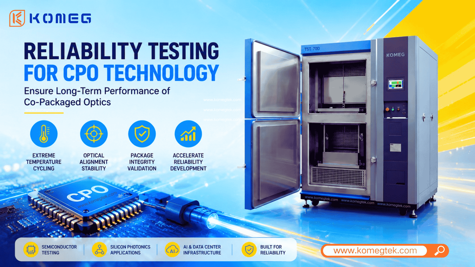
What Is a CPO Thermal Cycle Test Chamber?
A CPO thermal cycle test chamber is a programmable environmental testing facility designed to simulate repeated temperature fluctuations of CPO assemblies in actual operating environments. The equipment alternately exposes tested devices to high and low temperature conditions to accelerate thermal fatigue evolution, enabling manufacturers to detect latent structural defects before mass production and commercial application.
AI workloads generate continuous and irregular thermal fluctuations during operation, making thermal cycle testing indispensable for CPO qualification. The chamber enables manufacturers to conduct comprehensive evaluations on:
- Long-term optical stability
- Package structural integrity
- Solder joint reliability
- Fiber alignment stability
- Thermal durability of integrated components
Distinct from standard environmental test chambers, professional CPO testing systems are equipped with customized capabilities, including rapid temperature ramping, ultra-high temperature uniformity, low overshoot control, optical penetration ports, and real-time data monitoring. These specialized features make the equipment uniquely tailored for reliability verification in the semiconductor and silicon photonics industries.
Why Thermal Cycling Matters in Silicon Photonics
Silicon photonic devices are extremely sensitive to temperature variations. Slight thermal fluctuations can adversely affect optical wavelength, coupling efficiency, modulation performance, and overall signal integrity. In CPO architectures, optical components are tightly bonded to high-power ASICs, further exacerbating harsh thermal conditions.
With the continuous growth in power density of AI processors, thermal cycling stress inside CPO packages has intensified significantly. Modern AI accelerator clusters generate dramatic dynamic temperature changes during workload switching, GPU synchronization, power cycling, and burst data processing. Thermal cycle testing replicates these real-world operating conditions in a controlled laboratory environment, providing reliable data for product optimization and reliability validation.
Common Failure Mechanisms in CPO Systems
Fiber Misalignment
CTE mismatches between materials cause tiny displacements of optical components during thermal cycling. Even nanometer-level misalignment can elevate optical transmission loss, ranking fiber misalignment as one of the most critical reliability risks for CPO products.
Solder Fatigue
Repeated thermal expansion and contraction gradually fatigue solder joints. Long-term thermal cycling may trigger electrical instability, circuit open faults, and permanent mechanical damage. Complex heterogeneous integration structures make advanced semiconductor packages more vulnerable to solder fatigue failure.
Delamination
Thermal stress leads to interlayer separation of bonded materials within packages, which may occur between PIC layers, substrates, underfill materials, and thermal interface materials. Once delamination initiates, device performance will deteriorate at an accelerated rate.
Substrate Warpage
Large-scale advanced packaging substrates are prone to deformation under alternating temperature conditions. Substrate warpage negatively impacts optical alignment accuracy, mechanical structural integrity, and electrical connectivity, which has become a key concern for high-density AI packaging designs.
Laser Performance Degradation
Laser arrays feature high temperature sensitivity. Excessive thermal stress will undermine output power stability, cause wavelength deviation, and shorten service life. To mitigate thermal risks, some mainstream CPO architectures adopt external laser sources to isolate heat interference.
Typical CPO Thermal Cycling Conditions
Thermal cycling parameters are formulated based on product application scenarios and reliability qualification requirements. The mainstream testing temperature ranges include -40°C to +125°C and -55°C to +150°C. The conventional temperature ramp rates are set at 5°C/min, 10°C/min, and 15°C/min; higher ramp rates generate more severe thermal stress and accelerate fatigue failure.
Testing durations vary from hundreds to thousands of cycles, and some qualification tests require continuous long-term operation. Most semiconductor certification programs mandate real-time optical performance monitoring throughout the testing process.
Key Chamber Requirements for CPO Testing
Fast Ramp Rate Capability
AI and photonic systems undergo sharp temperature changes during operation. Therefore, CPO test chambers must support fast and stable temperature transitions to simulate thermal stress induced by actual workloads.
Excellent Temperature Uniformity
Uniform internal temperature distribution is essential to avoid localized thermal gradients that lead to inaccurate test results. This requirement is particularly stringent for large photonic packages, multi-chip modules, and silicon interposer systems.
Low Temperature Overshoot
Uncontrolled temperature overshoot may cause irreversible damage to sensitive optical devices. Precise PID temperature control is thus a mandatory configuration for professional CPO test chambers.
Optical Feedthrough Access
Real-time performance monitoring is required for most CPO validation tests. Advanced test chambers are equipped with optical feedthrough ports, fiber access interfaces, and data acquisition modules to continuously monitor BER, optical loss, signal integrity, and link stability during thermal cycling.
Long-Term Operational Stability
CPO qualification tests often last for days or even weeks. The test chambers must maintain stable airflow and precise temperature control to ensure uninterrupted long-term testing.
Thermal Shock vs Thermal Cycling for CPO
Both thermal cycling and thermal shock testing are core reliability verification methods for CPO. Thermal cycling features linear and controllable temperature ramping between extreme temperatures, while thermal shock testing realizes instantaneous temperature switching through hot and cold zone transfer.
Thermal shock chambers are applicable for intensive CTE stress assessment, accelerated solder fatigue analysis, and package robustness verification. In contrast, fast-ramp thermal cycling chambers are more suitable for evaluating optical stability and restoring real-world thermal operating characteristics of CPO devices.
Industry Standards Related to CPO Reliability Testing
A set of authoritative semiconductor reliability standards regulates CPO testing methodologies, mainly including JEDEC thermal cycling specifications, JESD22 reliability procedures, Telcordia optical reliability standards, and automotive semiconductor stress testing criteria. In addition, many manufacturers have developed customized internal testing protocols tailored for silicon photonics and AI infrastructure products.
Why AI Infrastructure Is Driving CPO Testing Demand
The booming construction of AI clusters has brought unprecedented demands for bandwidth and power density. Traditional electrical interconnection technology suffers from sharply declining efficiency at high data transmission rates. As a pivotal technology for scaling next-generation AI infrastructure, CPO has seen a rapidly expanding industrial application scale, which further raises requirements for environmental reliability testing. Future AI systems put forward higher standards for thermal stability, optical transmission speed, packaging density, and long-term service life, thereby driving a surging market demand for high-precision semiconductor environmental testing equipment.
KOMEG Environmental Testing Solutions for CPO Applications
KOMEG specializes in the R&D and manufacturing of high-end environmental testing equipment, providing professional reliability verification solutions for semiconductors and silicon photonics. The product portfolio covers fast ramp rate chambers, thermal cycle chambers, thermal shock chambers, temperature and humidity chambers, and customized semiconductor reliability testing systems.
KOMEG testing equipment is widely applied in semiconductor packaging validation, silicon photonics testing, optical module reliability assessment, and AI infrastructure durability verification. The core product advantages include precise temperature control, optimized airflow design, Ethernet data monitoring, USB data export, customized optical access ports, and semiconductor-grade temperature uniformity.
Future Trends in CPO Reliability Testing
With the continuous iteration of AI technology, CPO reliability testing standards will become more rigorous. The mainstream development trends in the industry are summarized as follows:
- Commercialization of 1.6T and 3.2T ultra-high-speed optical interconnections
- Continuously increased power density of AI chips
- Chiplet-based photonic integration technology iteration
- Upgraded 2.5D/3D advanced packaging technology
- Large-scale application of liquid-cooled AI infrastructure
- Popularization of optical input/output (I/O) architectures
Thermal management, packaging reliability optimization, and environmental stress validation will remain core technical challenges for next-generation AI infrastructure development.
Co-Packaged Optics has emerged as one of the most critical enabling technologies for future AI infrastructure and high-speed optical communication systems. Nevertheless, the heterogeneous integration of photonic and electronic components in compact packages brings prominent thermal reliability challenges. CPO thermal cycle test chambers play an irreplaceable role in verifying optical alignment stability, package durability, solder joint reliability, thermal fatigue resistance, and long-term operational performance.
Driven by the iterative upgrading of silicon photonics, AI accelerators, and advanced semiconductor packaging technologies, high-performance environmental testing equipment with fast temperature ramping, excellent uniformity, and precise control will become an indispensable infrastructure in the semiconductor industry.
KOMEG will continue to deliver high-quality environmental testing solutions to support reliability verification for semiconductors, silicon photonics, and AI infrastructure products.